

\ OVERVIEW
Bonding & sealing
Bonding joins the layers of a microfluidic device and seals them against leakage and contamination. It is the step that decides whether a chip works, and the one most often outsourced. A molder that can hold a 100 µm channel frequently cannot close one without destroying it. We run six polymer bonding methods — thermal fusion, solvent, laser welding, ultrasonic welding, UV adhesive and PSA lamination — plus hybrid joins to glass, silicon, membranes and films. We also bond parts made anywhere as a standalone service, from quantity one.


6
polymer bonding methods in house

> 0.6 MPa
pressure validated on production chips

0.5 µm
alignment with optical fiducials

10 materials
thermoplast, glass, silicon, PDMS — heteropairs

Qty 1
minimum order · ISO 13485 · FDA registered
\ CAPABILITIES
Capabilities and technical specifications
Six bonding methods in house, so the method is chosen for the material pair, channel depth and pressure rating — including the dissimilar pairs most bonding houses decline. Every lot is leak- and pressure-tested to the approved inspection plan, above 0.6 MPa on production chips.
Bonding methods compared
Four methods are direct — thermal fusion, solvent, laser welding and ultrasonic — and join the two polymers to each other with nothing in between. Two are intermediate — UV adhesive and PSA — and put a third material in the joint, which is what lets them join almost every pair on this page, dissimilar ones included — the matrix marks the exceptions.
Thermal fusion bonding— direct
Best for: microreactors
ADVANTAGES
Pure surface bonding with no additives. Maintains optical transparency. High bond strength, hermetic sealing, simple process
WHAT IT COSTS YOU
Slower cycle times. Limited scalability. Deformation risk. Process compatibility issues — destroys pre-applied surface chemistry
Ultrasonic welding— direct
Best for: POCT cartridges · microplates
ADVANTAGES
Short cycle times. Suited to batch processing. Effective for macro-scale cartridge assembly. Established, low-cost
WHAT IT COSTS YOU
Less accurate than other techniques. Needs custom fixtures. Rough bonding. Uneven energy distribution complicates melt-flow control
Solvent bonding— direct
Best for: droplet generators
ADVANTAGES
Clean full-surface bonding. High bond strength. Low process complexity. Adaptable across designs
WHAT IT COSTS YOU
Slow cycle times. Difficult to control. Potential chemical sensitivities. Environmental and safety considerations
UV-curable resin adhesive— intermediate
Best for: cell-culture microplates · cell-counting slides
ADVANTAGES
Rapid, scalable and suited to automated processes. Controlled adhesive layer thickness. High bond strength
WHAT IT COSTS YOU
Prone to channel blockage. Mixed materials in the joint. Limited channel-depth flexibility. Bubbles. Shrinkage deformation
Laser welding— direct
Best for: POCT cartridges · organ-on-a-chip · NGS · microplates
ADVANTAGES
No additives required. Short processing times. Highly accurate alignment. Bonds dissimilar materials
WHAT IT COSTS YOU
Thermal expansion at the weld area. Requires complex fixtures and clamping. Risk of warping from heat
Pressure-sensitive adhesive (PSA)— intermediate
Best for: reagent discs · microplates
ADVANTAGES
High bond strength, flexible, short processing times. Compatible with hydrophilic and hydrophobic coatings
WHAT IT COSTS YOU
Limited shelf life. Limited bond strength. Bubbles. Poor compatibility with some reagents
Alignment accuracy — two routes
This is the question we are asked most often. The choice is a cost decision more often than a capability one.
Mechanical alignment
ACCURACY
50 µm
HOW IT WORKS
Registration against pins, edges or features designed into the parts
REVERSIBLE
Yes — parts can be separated and re-registered
COST
Lower — no fiducials to design in, no alignment fixture per revision
CHOOSE IT WHEN
Channel-to-channel registration tolerance is loose relative to 50 µm, which covers most cartridge and manifold work
High-precision alignment
ACCURACY
To 0.5 µm
HOW IT WORKS
Optical alignment on fiducials, under a precision stage
REVERSIBLE
Bond-dependent
COST
Higher — setup, fixturing and cycle time all increase
CHOOSE IT WHEN
Electrode, optical or narrow-channel features have to land on each other, or a multi-layer stack accumulates error
vs
Validated performance
Pressure validated
> 0.6 MPa on production chips
PDMS bond strength
> 60 psi, glass-to-PDMS and PDMS-to-PDMS
Surface finish achievable
Ra 0.02 µm on bonded chip surfaces
Layer count
Up to 8 layers in PDMS; multi-layer in thermoplastic subject to method
Reversible bonding
Available on request where the device must be reopened — mechanically aligned assemblies separate most cleanly
Alignment accuracy
50 µm mechanical; to 0.5 µm with high-precision alignment
The rule that catches most programs.
Thermal and diffusion bonding run near the glass transition and will destroy pre-applied surface chemistry — immobilized antibody, dried reagent, functional groups. Either functionalize after bonding, or choose a lower-temperature method: solvent, adhesive or PSA. This is a design-stage decision. Discovering it at first article usually means remaking the part.
\ MATERIALS
Materials
Ten materials, direct and intermediate routes. Polymer-to-polymer bonding is the bulk of the work; hybrid joins to glass, silicon, membranes and films usually run through an intermediate layer.

SCOPE
Polymer bonding — plastic to plastic, the six methods above
WHERE IT IS DESCRIBED
This page. It is the bulk of the work we do

SCOPE
Silicon and glass wafer bonding — anodic, fusion, wafer-level
WHERE IT IS DESCRIBED

SCOPE
Hybrid bonding — plastic to glass, plastic to silicon, plastic to membrane or film
WHERE IT IS DESCRIBED
The compatibility matrix below

SCOPE
Intermediate-layer bonding — UV adhesive, PSA
WHERE IT IS DESCRIBED
Near-universal. It joins almost every pair on this page, which is why it is the fallback whenever a direct bond is not available; the matrix marks the few exceptions
Which materials bond to which
D = direct bond · I = intermediate, using an interlayer or adhesive.
✓ standard △ feasible ✗ unsupported
MATERIALS
PMMA
✓
✓
△
✓
△
✓
△
△
△
✓
△
✓
✗
△
✗
✓
✗
✓
✗
✓
D
I
D
I
D
I
D
I
D
I
D
I
D
I
D
I
D
I
D
I
PC
PMMA
PS
PP
COC
COP
PDMS
GLASS
SILICON
PI
PC
△
✓
✓
✓
△
✓
△
△
△
✓
△
✓
✗
△
✗
✓
✗
✓
✗
✓
PS
△
✓
△
✓
✓
✓
△
△
△
✓
△
✓
✗
△
✗
✓
✗
✓
✗
✓
PP
△
△
△
△
△
△
✓
△
△
△
△
△
✗
✗
✗
△
✗
△
✗
△
COC
△
✓
△
✓
△
✓
△
△
✓
✓
✓
✓
✗
△
✗
✓
✗
✓
✗
✓
COP
△
✓
△
✓
△
✓
△
△
✓
✓
✓
✓
✗
△
✗
✓
✗
✓
✗
✓
PDMS
✗
△
✗
△
✗
△
✗
✗
✗
△
✗
△
✓
△
✓
✓
✓
✓
✗
△
Glass
✗
✓
✗
✓
✗
✓
✗
△
✗
✓
✗
✓
✓
✓
✓
✓
✓
✓
✗
✓
Silicon
✗
✓
✗
✓
✗
✓
✗
△
✗
✓
✗
✓
✓
✓
✓
✓
✗
✓
✗
✓
PI
✗
✓
✗
✓
✗
✓
✗
△
✗
✓
✗
✓
✗
△
✗
✓
✗
✓
✓
✓
A pair marked ✗ under D and ✓ under I is not a problem.
It means the join needs an interlayer, which is routine. What matters is whether the interlayer is acceptable in your fluid path — that is a DFM question, and usually the first one we ask.
The column most suppliers cannot fill.
Dissimilar plastic-to-plastic direct bonding — COC to PMMA, PC to PS — is the hardest part of the matrix, and the reason chips arrive here from other manufacturers for this step alone. If your device joins two different thermoplastics with no adhesive permitted in the fluid path, that is the conversation to start with.
Direct vs. intermediate bonding
Which family a method belongs to decides what ends up in the joint. Grade-level material data is in the Materials guide.
Direct — fusion · solvent · laser · ultrasonic
WHAT IS IN THE JOINT
The two polymers themselves, nothing in between
MATERIAL PAIRS
Same-polymer pairs as standard; dissimilar pairs feasible for selected combinations (see matrix)
WHAT THE FLUID TOUCHES
Only the two polymers
PRE-APPLIED SURFACE CHEMISTRY
Thermal fusion destroys it; solvent is the lower-temperature direct route
Intermediate — UV adhesive · PSA
WHAT IS IN THE JOINT
A third material — cured resin or an adhesive film
MATERIAL PAIRS
Almost every pair on this page, including plastic to glass, silicon, membrane or film — see the matrix for the exceptions
WHAT THE FLUID TOUCHES
The interlayer — mixed materials in the joint; PSA has poor compatibility with some reagents
PRE-APPLIED SURFACE CHEMISTRY
Lower-temperature — adhesive and PSA are the usual routes when the surface is already functionalized
vs
\ PROCESS
Bonding process
The method is chosen for the device; the workflow that proves the bond is the same for all six.
Method selection

Material pair and requirement
We take the two materials, the channel depth, the pressure rating and any surface chemistry already applied. We accept parts made anywhere.
Quantity one accepted

Method selection and DFM
We choose the method against those constraints, not against our equipment. At this step we flag anything that will not hold — channel depth too shallow for fusion, an interlayer the reagent will not tolerate.
6 methods · free DFM review
DIRECT
Thermal fusion
No additives, hermetic, transparency kept — for deep channels with no surface chemistry applied yet.
DIRECT
Ultrasonic welding
Short cycles, batch-friendly, low cost — macro-scale cartridge assembly where precision is not the constraint.
DIRECT
Solvent bonding
Clean full-surface bond, low process complexity — droplet generators; slow and chemistry-sensitive.
INTERMEDIATE
UV-curable adhesive
Rapid, automatable, controlled layer thickness — microplates and cell-counting slides.
DIRECT
Laser welding
No additives, accurate alignment, dissimilar materials — POCT cartridges, organ-on-a-chip, NGS.
INTERMEDIATE
PSA lamination
Short processing time, compatible with hydrophilic and hydrophobic coatings — reagent discs and microplates.
Common workflow
Once the method is chosen, every device runs the same five steps.
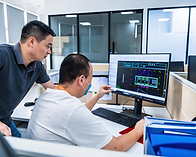
Fixture fabrication
Bonding fixtures designed and made for your geometry — included in the standalone lead time.
Inside the 2–3 weeks

Alignment
Mechanical registration against pins, edges or designed-in features; optical alignment on fiducials where the tolerance demands it.
50 µm mechanical · 0.5 µm optical

Parameter tuning and bonding
Temperature, pressure and dwell developed on your actual parts, then a sample run before production.
Up to 10 sample pieces

Leak and pressure test
Leak and burst testing to the approved inspection plan; bond quality is measured on the finished assembly, not inferred from the recipe.
> 0.6 MPa validated

Release and packaging
Released against the acceptance criteria; individually packaged in PE bags or sterile self-sealing pouches.
PE bag or sterile pouch

\ QUALITY CONTROL
Quality control

Bonding inspection
Visual and dimensional inspection against the approved drawing — voids, channel deformation, adhesive wicking
Leak testing
To the approved inspection plan and acceptance criteria
Additional testing
Tensile and pull-force, fluidic performance, protein adsorption where the application requires it
Alignment
50 µm on mechanically registered assemblies; to 0.5 µm with optical alignment on fiducials
Pressure testing
Burst and pressure resistance; > 0.6 MPa validated on production chips
Quality system
ISO 13485 certified · FDA registered · ISO 7 cleanroom
\ LEAD TIME & MOQ
Lead time & MOQ

Lead time
2–3 weeks as a standalone service

Delivery
Individually packaged in PE bags or sterile self-sealing pouches

What that covers
Bonding fixture fabrication, bonding parameter tuning, and up to 10 sample pieces — proving the bond, not just performing it

Indicative pricing
NRE from $2,000 — fixture, parameter development and the sample run; a familiar material pair sits at the floor, a new pair or a multi-layer stack above it

Minimum order
Quantity one accepted; parts made anywhere
The lead time includes proving the bond.
Fixture design and parameter development happen within the two to three weeks — you do not pay for a development phase and then wait again for parts. If your current vendor is struggling with bond yield, leak rate or channel deformation, that is a two-to-three-week conversation, not a requalification. Nothing else in your supply chain changes.
\ SHOWCASE
Case studies and applications
Sample parts
A program where four of the six methods ran on one platform.
Microfluidic LNP synthesis platform
Lipid nanoparticle synthesis moved from batch processing to continuous, automated production — integrating MEMS fabrication with thermoplastic chip manufacturing, and using four bonding methods on a single platform.


THE CHALLENGE
Manufacturing pain points
High PDI variation in traditional batch synthesis. A scale-up gap from lab to commercial GMP volumes. Reagent loss and inconsistency in manual mixing. Pharma-grade traceability and validation burden.

SOLUTION
Integrated microfluidic platform
PDMS prototyping to COC commercial chip pathway. MEMS microstructures with sub-micron channel control. Multi-bonding — thermal, ultrasonic, laser and solvent on one platform. Continuous-flow lipid–aqueous mixing architecture.

DELIVERED
Validated production outcomes
Reproducible particle size with tight PDI control. Lab-to-commercial scale-up with no requalification. Ra 0.02 µm surface and > 0.6 MPa pressure validated. ISO 13485 / ISO 7 cleanroom-manufactured chips.
Applications
LASER · ULTRASONIC
POCT cartridges welded without additives — the fluid path stays the molded polymer, at consumer unit cost.
LASER WELDING
Flow cells where optical transparency and surface chemistry inside the well must survive the bond.
LASER WELDING
Dissimilar layers and membranes joined with accurate alignment and no adhesive in contact with the culture.
SOLVENT BONDING
Droplet generators closed by clean full-surface bonding, so the junction dimensions and wall chemistry are the ones that were designed.
FAQ


