
High-Performance Glass Microfluidics
At HICOMP, we specialize in the custom design, rapid prototyping, and contract manufacturing of high-performance glass microfluidic devices. Utilizing advanced femtosecond laser micromachining, we overcome the limitations of conventional etching to deliver complex 3D architectures with sub-micron accuracy across all glass types.
Whether you are developing platforms for Next-Generation Sequencing (NGS), Single-Cell Analysis, Point-of-Care (PoC) Diagnostics, or EWOD applications, our expertise ensures ultra-clean results with superior optical clarity and chemical resistance.
Specialized Product Applications


Diagnostics & Genomics
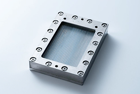
High-transparency Flow Cells designed for Next-Generation Sequencing (NGS) and consistent fluid control.
Cell Biology
Specialized Single-Cell/Single-Molecule Analysis chips featuring microwell and pillar arrays for high-sensitivity research.
Digital Microfluidics
EWOD (Electrowetting-on-Dielectric) chips with engineered substrates for precise droplet manipulation.
Chemical Synthesis
Robust Flow Reactors with multi-layer designs and high bonding strength capable of withstanding harsh conditions.
Device Manufacturing Capabilities

We offer:
-
Glass Micromachining: High-resolution Dry/Wet etching and glass micro-molding with feature sizes as small as 1 μm.
-
Precision Laser Drilling: Specialized laser drilling for high-aspect-ratio holes with edge-chipping controlled to < 5 μm.
-
Advanced Glass Bonding: Direct and intermediate-layer bonding with industry-leading alignment accuracy of ≤ 10 μm.
-
Patterned Electrodes: Integration of precision electrodes directly onto glass substrates for active fluid control.
Technical Spec and Device Features
Glass microfluidics are essential across diverse sectors, including high-throughput NGS, single-cell and single-molecule analysis, point-of-care diagnostics, and advanced flow chemistry.
While we provide the flexibility to investigate other materials such as silicon and PDMS, glass remains the gold standard for applications requiring superior optical clarity, chemical inertness, and mechanical stability. The ideal material selection is always driven by your specific application requirements, solvent compatibility, design complexity, and project budget.
Microstructure
-
Substrate Thickness: 0.1 - 2.0 mm
-
Thickness Uniformity: +/- 5 μm
-
Surface Roughness (Ra): < 2 nm
-
Channel Size: Length ≥ 50 μm, Width ≥ 10 μm
Microwell
-
Feature Size (Well/Pillar): Down to 2 μm
-
Aperture Diameter: > 0.1 μm
-
Aperture Uniformity: CV < 5%
-
Aspect Ratio: < 10
-
Tilt Angle: 80 - 90 degrees
-
Hole Pitch: > 0.1 μm
Glass Drilling
-
Aperture Diameter: 0.1 - 10 mm
-
Edge-chipping Size: < 5 μm
-
Taper Control: Upper/Lower difference < 10%
-
Position Accuracy: ± 25 μm
Bonding
-
Bonding Process: Laser bonding, UV bonding, Anodic bonding, or PSA bonding
-
Alignment Accuracy: 50 μm
-
Material Combinations:
-
Glass-to-Glass Bonding
-
Glass-to-Silicon Bonding
-
Glass-to-Polymer/Plastic Bonding
-

Laser Drilling

Patterned Electrodes

Glass Microchannel

Glass Micro-well/pillar Array
TGV Laser System
.png)
FLEE-TGV is a femtosecond-laser-enhanced glass via processing platform designed for high-precision through-glass microstructures and advanced glass microfluidic fabrication.
Glass substrates are increasingly used in advanced packaging, life-science devices, and microfluidic systems where high-aspect-ratio vias, blind holes, and complex microchannels are required. The FLEE-TGV system integrates femtosecond laser processing with post-etch enhancement to enable efficient and high-quality fabrication across a wide range of glass materials and structure geometries.
With independently developed processing and control technologies, automatic wafer calibration capability, and fully automated operation, the platform supports scalable manufacturing of straight vias, tapered vias, conical holes, and special-shaped microstructures for applications including advanced packaging, display manufacturing, consumer electronics, and life-science glass microdevices.
Main Features
-
Flexible substrate compatibility, supporting wafer sizes up to 300 mm
-
Femtosecond laser processing for high efficiency and high precision
-
Independently developed processing and motion control system
-
Integrated high-precision wafer automatic calibration
-
Fully automated operation workflow
-
Proprietary core technologies with independent intellectual property
Parameters
-
Wafer size: 4 inch – 12 inch
-
Glass thickness range: 0.1 mm – 1 mm
-
Processing efficiency: ≥ 5000 holes/s
-
Maximum aspect ratio (depth/diameter): ≥ 50:1 (material-dependent)
-
Minimum aperture diameter: < 5 µm (material & thickness dependent)
-
Taper angle: 1° – 10° (material-dependent)
-
Positioning accuracy: ± 5 µm
Case Studies

Flow Focusing & Cell Sorting Chip(d=62μm)

Micro-Difusion Mixer Chip ( d=40μm )
Customer Challenge
-
Microstructure Precision: Need for complex feature sizes down to 1 um and microwell arrays down to 2 um.
-
Optical Standards: Requirement for high-transparency substrates with surface roughness Ra less than 2 nm for molecular analysis.
-
Strict Alignment: Necessity for bonding alignment accuracy of 10 um or less for multi-layer designs.
-
Structural Quality: Risk of edge-chipping during custom form factor cutting; must be kept under 5 um.
Engineering Approach
-
Integrated Machining: Combined dry/wet etching with micro-glass molding for high-efficiency feature creation.
-
Thermal Molding Cycle: Implemented a four-stage process involving heating, pressing, annealing, and cooling.
-
Laser Integration: Utilized precision laser drilling for apertures between 0.1 and 10 mm with controlled taper.
-
Advanced Bonding: Deployed Laser, UV, Anodic, and PSA bonding techniques to accommodate various material combinations.
Manufacturing Outcome
-
High Resolution: Achieved feature sizes down to 1 um and channel widths of 10 um or greater.
-
Complex Geometries: Successfully produced specialized Microlens, Micropyramid, and Microcylindrical arrays.
-
Quality Control: Maintained position accuracy within 25 um and aperture uniformity within a 5% coefficient of variation.
-
Versatile Applications: Delivered production-ready chips for NGS, single-cell analysis, EWOD, and flow reactors.