\ OVERVIEW
Product design & DFM
We offer three design services. Complete product design — the reader instrument and the cartridge it runs, designed as one system — for at-home test products. Chip design for any application, on two routes. Design support is for teams with a schematic and engineers of their own; full development runs from the assay to a verified device, with the IP position handled. And DFM review, which is complimentary. A six-stage program takes a concept to commercial production, with the manufacturing route chosen at the start rather than discovered at tooling.


3 services
product design · chip design · DFM review

2 routes
chip design: design support or full develop

2–4 weeks
to requirement assessment & design proposal

500+
projects delivered

ISO 13485
certified · FDA registered
\ CAPABILITIES
Scope and deliverables
We manufacture what we design, so the DFM report is written against our own tooling and yield, and the prototype, the pilot mold and the production mold come from one team. Every process is available at stage one, and each stage states the monthly chip volume it reaches before you commit.
What we design
Complete product design
WHAT IT COVERS
At-home test products only — the reader instrument and the cartridge it runs, designed as one system so the detection, the fluidics and the user interaction are settled together
WHAT WE NEED FROM YOU
The assay, the intended user and the intended use environment
HOW IT IS CHARGED
Quoted per program
Chip design
WHAT IT COVERS
Microfluidic chip architecture across any application — the channel layout, the geometry and the process route that will make it. Two routes, below
WHAT WE NEED FROM YOU
A workflow (the one item we cannot start without — a hand sketch of the steps is enough), the assay, and reference literature where it exists
HOW IT IS CHARGED
Fixed fee, or from $200,000 for full development
DFM review
WHAT IT COVERS
Manufacturability assessment of a design against the process it will actually be made in: what holds, what does not, and what changing it costs
WHAT WE NEED FROM YOU
CAD and a 2D drawing
HOW IT IS CHARGED
Complimentary
Why complete product design is scoped to one product type.
Designing a reader and its cartridge together is a systems problem: detection, fluidics, mechanics, user handling and manufacturing cost all move against each other. At-home tests are where we have done it before. For every other application, the useful division is that the chip is ours and the instrument is yours.
Chip design — design support vs. full development
The route depends on how much design already exists, and on whether you want the intellectual-property position handled as part of the work.
Design support
WHO IT IS FOR
You have a preliminary design or schematic, and engineering capability of your own
WHAT YOU RECEIVE
Your concept developed through to a manufacturable CAD file, with DFM
VERIFICATION
Yours to run
PRIOR ART / FREEDOM TO OPERATE
Not included. We design to your specification; the design is not warranted free of third-party rights — that stays with you and your counsel
PATENTS
None filed
FEE
Fixed fee, estimated and approved before anything starts — no hourly meter, no invoice you have not already seen
CREDITED AGAINST MANUFACTURING
—
Full development
WHO IT IS FOR
You have an assay and an intended product, and no device design
WHAT YOU RECEIVE
Concept to verified device: architecture, CAD, prototypes, design iterations, verification builds and the IP position
VERIFICATION
Included — it runs on our own manufacturing, which is why the two are quoted together
PRIOR ART / FREEDOM TO OPERATE
Included — prior-art search and freedom-to-operate opinion by registered patent counsel
PATENTS
One or more US applications, drafted and prosecuted by patent counsel. Inventors named as the law requires; all rights assigned to you
FEE
From $200,000, beginning with a $15,000–30,000 Phase 0 feasibility study
CREDITED AGAINST MANUFACTURING
Part of the design fee is credited against production
vs
Phase 0 exists so that nobody commits $200,000 to a plan.
It produces two or three candidate architectures, the manufacturing route each one implies, a first read of the patent landscape, and a costed plan for the full program. If the device should not be built the way you imagined, you learn that for the price of Phase 0.
How the IP works on full development.
Patent work is performed by registered patent counsel that we engage and manage — HiComp does not itself practice before the USPTO. Inventorship is determined by who actually conceived the invention, as US law requires, so where our engineers contribute they are named; every right they hold is then assigned to you. You own the patent. Counsel and USPTO fees are quoted and passed through at cost, separately from the program fee, so neither side is exposed to how many office actions a case attracts.
\ MATERIALS
Materials
Material and process are one decision, and it is made in Stage 1. The prototyping route and the volume route have to be compatible, or the program pays for the design twice.

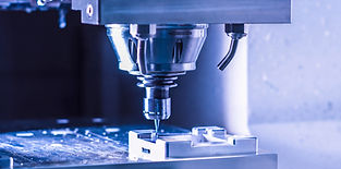
Injection-molded COC/COP or PC → CNC micro milling or 3D-printed inserts in the same resin
WHY THIS PAIRING
Machined in the production resin, so optical and chemical behavior is real from the first test
WHERE IT BREAKS
Draft, wall thickness and shrink do not exist in a machined part — they have to be designed in before tooling

PDMS at volume → Soft lithography on SU-8, then a closed mold
WHY THIS PAIRING
Identical material at both ends; only the forming method changes
WHERE IT BREAKS
Open-cast tolerances are looser than closed-mold production — expect the transfer step

Glass → Etched glass at wafer scale
WHY THIS PAIRING
Same substrate, process and bonding route — prototype and production differ only in wafer count
WHERE IT BREAKS
Volume scales by batching wafers, not by tooling, so unit cost falls more slowly than in a molded part

A hybrid construction → The layer that carries the function first
WHY THIS PAIRING
Establishes whether the biology or the detection works before the assembly problem is added
WHERE IT BREAKS
Bond compatibility between the layers is the constraint, and it is easiest to fix on paper
Every substrate compared, grade by grade, is in the Materials guide; all eight processes side by side are on the services overview.
Design rules by route
What each prototyping and production route will actually hold. Design to the route you intend to scale in.
3D printing — two-photon
MINIMUM FEATURE
Sub-micron
TOLERANCE
Process-dependent
TOOLING
None
SENSIBLE QUANTITY
1–50
Glass — DRIE and laser
MINIMUM FEATURE
1 µm
TOLERANCE
Process-dependent
TOOLING
Photomask
SENSIBLE QUANTITY
One wafer upward
3D printing — DLP
MINIMUM FEATURE
~2 µm
TOLERANCE
Process-dependent
TOOLING
None
SENSIBLE QUANTITY
1–200
MEMS wafer process
MINIMUM FEATURE
2 µm
TOLERANCE
Wafer-scale
TOOLING
Photomask
SENSIBLE QUANTITY
One wafer upward
CNC micro milling
MINIMUM FEATURE
~100 µm channel width
TOLERANCE
±0.05 mm standard; ±0.02 mm high precision
TOOLING
None
SENSIBLE QUANTITY
1–500
Cleanroom injection molding
MINIMUM FEATURE
> 500 µm general features; replicated microchannels 10–200 µm
TOLERANCE
Typically ±0.30 mm or tighter by feature
TOOLING
Production mold
SENSIBLE QUANTITY
500 upward
PDMS soft lithography
MINIMUM FEATURE
~5 µm
TOLERANCE
Mold-limited
TOOLING
SU-8 master
SENSIBLE QUANTITY
20–5,000
The most costly design error we see is a molded part designed as though it were a machined one.
Draft angle, uniform wall thickness, gate position, knit lines and shrink have no equivalent in a milled prototype, and they decide whether the tool can be filled. If the product will be molded, the molding rules apply from the first CAD file.
\ PROCESS
Design process
Six stages from first conversation to commercial supply. Durations are typical for a device of moderate complexity and run from sign-off of the previous stage; Stages 4 and 5 frequently overlap.

Concept and requirement definition
Define the application scenario and the core functional requirements — throughput, detection principle, sample type. Ends with a requirement assessment report and an initial design proposal.
2–4 weeks · documentation only

Chip design and prototype development
Complete the chip structure design; produce the first SU-8 molds and PDMS or CNC prototypes as functional verification chips.
2–4 weeks · 20–50 chips/month

Function verification and optimization
Iterate design and verification until the core functions meet the requirement. We iterate; you test on your own assay; the loop repeats.
2–3 months · 50–200 chips/month

Process finalization and pilot production
Establish stable bonding, packaging and surface treatment; deliver consistent small batches; develop pilot molds.
3–5 months · 200–1,000 chips/month

Mass-production preparation
Develop production molds and validate large-scale feasibility before production tooling is released.
3–5 months · 1,000–5,000 chips/month

Commercial production
Stable, continuous supply against commercial demand under a long-term supply agreement.
Ongoing · ≥ 10,000 chips/month
What each side does
The division of labor follows your request. By default you keep the biology and the IP, and we build the device and the process that makes it repeatably; where you want it, we build the chip and the biology too, as a full-service program.
↓ YOU RECEIVE
↓ YOU PROVIDE
Stage 1–2
Application background, workflow, assay, literature and patent references, key requirements, testing requirements, design sign-off
Requirement assessment report, initial design proposal, CAD drawings, SU-8 molds, first functional verification chips
Stage 3
Experimental testing on your own assay, and feedback
Multiple design iterations, test reports, optimization plans
Stage 4–5
Confirmation of the process plan, target testing conditions, mold structure and QC acceptance criteria
Process documentation (SOPs), consistency reports, stable small-batch product, pilot molds, production molds, process validation reports, quality inspection plans
Stage 6
Long-term supply agreement, rolling forecast, regular market and application feedback
Mass-produced chips, full QC documentation, packaging and delivery
End to end, a device of moderate complexity takes roughly nine to fifteen months from first conversation to commercial production.
Most of that is not drawing; it is the verification and process-stabilization work in Stages 3 and 4, where a design either becomes manufacturable or does not.

\ QUALITY CONTROL
Stage gates

Stage gate
Each stage begins on written acceptance of the previous deliverable — what keeps a redesign from arriving after tooling
Verification data
Test reports at each Stage 3 iteration, against the acceptance criteria agreed in Stage 1
Process validation
Formal validation and an inspection plan in Stage 5, before production tooling is released
Quality system
ISO 13485 certified · FDA registered
DFM report
Issued against the CAD before any mold or master is cut: what will hold, what will not, what it would cost to change
Consistency reports
Batch-to-batch data in Stage 4, before the process is called stable
Documentation
SOPs, validation reports and inspection plans produced under ISO 13485 as the work happens
Design history is easier to keep than to reconstruct.
If the device is heading for a regulatory submission, we generate the documents that submission needs at the stage they belong to. Rebuilding a design history file two years later from emails and CAD revisions is the expensive way to do it.
\ LEAD TIME & MOQ
Fees, timelines and IP
Fees

DFM review
Complimentary

Credited against manufacturing
Part of the full-development design fee is credited against production

Chip design — design support
Fixed fee, estimated and approved before work begins

Patent costs
Counsel and USPTO fees quoted and passed through at cost, separately from the program fee

Chip design — full development
Phase 0 feasibility study $15,000–30,000; full program from $200,000

Complete product design
Quoted per program
Timelines

Requirement assessment & proposal
2–4 weeks

First functional chips in hand
2–4 weeks after design sign-off

Verified design to validated tooling
2–3 months, then 3–5 months each for pilot and production tooling, frequently overlapping

Phase 0 duration
2–4 weeks
What you own
The design
Yours — the device design, the application and the data

The patents
Yours, on the full development route — every right held by our engineers is assigned to you

Your biology
Stays with you — we do not run your assay or hold your compounds, reagent formulation or clinical data

What HiComp retains
Our own process knowledge — how a geometry is molded or bonded — not specific to your product
\ SHOWCASE
Case studies and applications
COMPLETE PRODUCT DESIGN
The one product type where we design the reader and the cartridge together.
DESIGN → TOOLING
SBS-format plates designed for the mold from the first CAD file.
CHIP DESIGN
Device design in PDMS or hybrid construction, with the biological model developed alongside.
ROUTE CHOSEN EARLY
Partition arrays where the prototyping and volume routes must be compatible from Stage 1.