
-
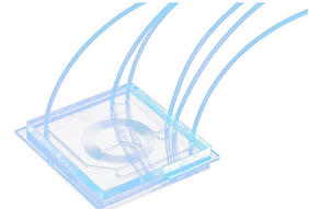
HiComp delivers production-grade PDMS devices with a clean finish, precise thickness control, and injection molding level quality.
-
Support organ-on-chip, organoids, cell culture, diagnostics, liquid biopsy, and drug discovery with speed and industrial-scale yield.
Applications


Process flow -Lab vs. HiComp at Scale
Typical Lab Setup
HiComp Production

Manual weigh & hand-mix; variable degassing
Metered mixing and controlled vacuum degassing in dedicated equipment for bubble free bulk PDMS and batch-to-batch consistency.
2.PDMS Mixing
4.Bonding

6.Assembly


Benchtop tubing; manual assembly
Single-piece plasma bonding by hand
Batch bonding in fixtures and high yield.
Documented assembly (tubing, membranes, electrodes) or cartridge integration for high-volume packaging.


1.Master Mold
SU-8 photoresist on wafer; open tool; limited lifetime
Mother mold Tooling by using 3D printing, CNC, SU-8, and silicon etch; long-life resin master for batch fabrication.
3.Casting / Molding
Open cast on wafer; thickness & flatness vary
Closed-mold PDMS molding with calibrated pressure for thickness, planarity, and surface finish control.
5.Ports & Reservoirs
Manual punch/drill; debris & misalignment risk
Molded-in ports/reservoirs (no punching) or precision drilling with capture & clean protocols.
When to use which
-
Prototype & small batches (1–100 pcs/order): lab-style or hybrid for speed.
-
Pilot/bridge (100–500 pcs/order or <500 pcs/month): hybrid with selected closed-mold steps to boost yield.
-
High volume (≥500 pcs/month): HiComp closed-mold production for repeatability, cost, and scale.
HiComp PDMS Capabilities
Geometry & Features
Minimum channel width: ≥ 2 µm
Channel depth tolerance: ±5%
Channel aspect ratio: up to 10:1
Minimum through-hole diameter: 0.30 mm
Maximum chip size: up to 300 mm × 300 mm
QC& Logistics
-
Cleanroom: ISO 7 protocols
-
Particle control: microscopic inspection; debris-free in critical areas
-
Lead times: 2–3 weeks after design confirmation (expedites available)
-
MOQ: no strict MOQ; pricing improves with batch size
-
Maximum monthly capacity: up to 80,000 pcs/month
-
Deliverables: bare chips, chips with pre-assembled tubing,
or fully integrated cartridge assemblies
Layers
-
Layer count: 2–8 layers
-
Alignment accuracy (typical): 0.10 mm (tighter available on request)
-
Thickness tolerance: up to ±5 µm (design-dependent)
-
Flatness: as low as 2 µm, maintained via closed-mold planarity controls
-
Color/tinting: clear (default) or tinted/colored PDMS
Bonding & Integration
-
Bonding options: bubble-free glass/PDMS and PDMS/PDMS bonding
-
Bond strength: > 60 psi
-
Temporary/reversible bonding: available on request
-
Integrated features: molded-in through-holes/reservoirs
-
Membranes & electrodes: bonded membranes; embedded electrodes supported


Why Choose Us

Integrated Mold
Closed mold, NOT SU-8 wafers.
Precise Molding
Molded, NOT casted.

Scalable Pipeline
By technicians, NOT scientists.

ISO 7
Cleanroom

ISO 13485
Certified

FDA
Registered

1M+ PDMS
Chips Delivered

Trusted by
Global Leaders